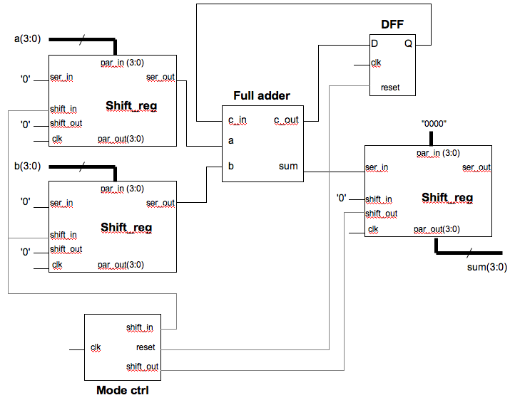
The above block diagram describes a digital design that demonstrates bit-serial arithmetic. Two 4-bit parallel inputs are converted to 4-bit serial bit streams with least significant bit (LSB) first. A full-adder sums the two numbers on bit at a time, carrying-in the carry bit from the previous clock cycle. Finally the output serial bitstream is converted back into a parallel sum. To build this circuit, several separate components must be created and verified in simulation.
Shift Register:
You need to produce a dual-purpose shift register that can:
If the shift_in signal is set to 1, the four bits of parallel input data are loaded from par_in into the 4-bit register. If the shift_out signal is set to 1, the contents of the shift register are clocked into a second four-bit register connected to par_out.
Design the shift register and test all functionalities.
D flip-flop (DFF):
A single register (flip-flop) is needed to save the carry-out from the full adder after each clock cycle
and present it to the carry-in at the start of the next clock cycle. The register timing should use the
rising edge of the clock, and have a synchronous reset (If reset='1' the value of Q is set
to '0' at the next rising edge, otherwise Q is set to the value at input D.)
You can either create a separate component for the DFF, or simply implement it as a clock-dependent process in the top-level design.
Full Adder:
You may either use the full adder that you designed in Lab 1, or write
a new, simpler version as a single entity and architecture. If you
choose the former option, make sure that the vhdl files for all of the
components are copied into your new project, so that you can
change them (as needed) without affecting the other design
Mode_control:
This is a state machine with a single clock input (clk), that produces three output signals that
control the relative timing of the different component (shift_in, shift_out and reset).
Each of these outputs is set high (1) for one clock cycle, and low (0) for the other three.
New data are read in by the input shift registers when shift_in is equal to 1. For the next three cycles the contents of the register are shifted out one at a time and sent to the adder.
The reset signal is used to prevent the carry-out of the top-most bits in the summation from being carried in to the next calculation. When reset is set high, the output of the DFF is forced to '0'.
The contents of the output shift register are properly aligned once every four clock cycles, just after a four bit summation is completed. At this time, the shift_out signal is set to 1, and the correctly aligned result is held on ser_out to be sent to the display.
The mode_control state machine should have four states, with the three outputs correctly defined for each state. Simulate the mode-control block separately to show that it produces a repeating sequence of the three control signals. When you integrate the final design you may need to adjust the relative timing of the signals to make the adder work properly.
Serial Adder:
Once you have written and simulated each of the individual components, instantiate them in a top-level architecture
resembling the figure above. Simulate, and adjust the timing of the mode_control component until the
adder works correctly. Pay special attention to the carry chain and the alignment of the output.
Once the simulation works, implement it in your developer board. Use eight switches for the two four-bit inputs, and four LEDs to display the output.
For timing, use the 100 MHz oscillator clock supplied to pin W5 of the FPGA.
If time permits, you can implement the output as numbers using the seven-segment LED display. This can be done by instantiating the VHDL module disp4.vhd (<- downloadable from this page on the course site) and modifying the pin constraints accordingly. Only one digit is needed (four bits) to display the result, so the other 12 input bits of the disp4 module should be set to '0'.