Lab 7
Arbitrary Function Generator
Introduction
In this project, you will implement an analog function generator
with selectable square, triangle or sine wave output.
The project uses the peripheral module PMOD DA1.As a starting point,
there is a pre-made VHDL control interface for this module
(pmod_da1_ctrl.vhd) available for download from the course
web page.
Documentation for the PMOD DA1 module (in PDF form) is also available
on the web page.
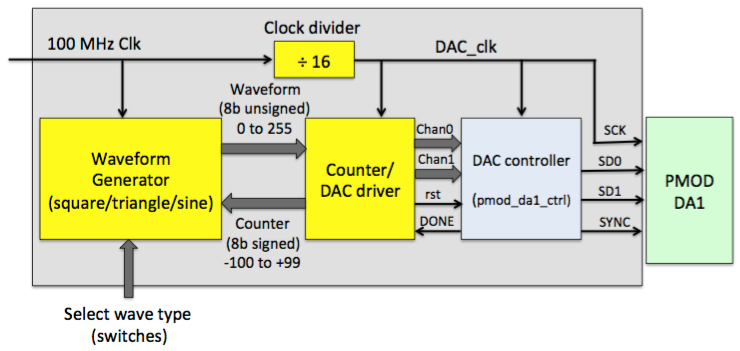
Design overview
A suggested design is shown in the above block diagram. Here,
the functionality is divided between two main blocks. These may be
implemented as separate VHDL components, or processes in the main
architecture.
- Waveform Generator: Receives an 8-bit signed counter value
(range -100 to +99), and from that value calculates an 8-bit unsigned DAC
output (range 0 to 255). The generator can produce square, triangle and
sine wave forms, and user switches are used to select the desired output.
- Counter/DAC driver: Receives the 8-bit unsigned output
from the Waveform Generator, and transfers it to pmod_da1_ctrl using
a simple protocol. This functional block also contains the 8-bit
signed counter that drives the input of the Waveform Generator. The
counter is incremented once per write cycle to the DAC.
The Waveform Generator can (and should) run at the 100 MHz system
clock rate. The PMOD_DA1 cannot run at higher than 25 MHz, and the
BASYS3 PMOD pins have additional limitations, so a clock divider is
necessary to produce a slower DAC_clk. This slow clock also drives the
pmod_da1_ctrl component and the Counter/DAC driver block.
For simplicity, the output frequency and amplitude can be fixed to
single values. More details are given in the following sections.
Waveform generator
The waveform generator receives a single 8-bit signed "X" input with range
-100 to -99, and produces a corresponding "Y" value
(8 bit std_logic_vector in unsigned notation) for a square wave,
triangle wave, and sine (or cosine) wave at that value of "X". The
desired "Y" value is selected for output by some combination of user
switch inputs. You can decide the best way to implement this
interface. You may also implement the different waveforms as you like,
but the following are some suggestions for how this could be done.
Square wave
A square wave is trivial to implement. Since the counter input range
is -100 to +99, one simple approach would to set the output
value low (0) if X is negative, and high (255) if X is positive.
Triangle wave
The triangle wave is slightly more complicated to produce than the
square wave, because it has a continuously rising value for half of
the cycle, and a falling value for the other half.
You can still take advantage of the fact that the counter input
alternates between negative and positive. For instance, a simple
triangle wave can be made by setting Y=X when X is positive, and
Y=100+X when X is negative. Convert the result to an 8-bit std_logic_vector.
This strategy will create an output range of only 0-100 (the full scale is
255), which is less than ideal. You can easily multiply the
output scale by 2 (0-200) by "left-shifting". In other words, truncate the
MSB of the vector, and concatenate an extra '0' bit to
the LSB end of the vector.
Sine (or cosine)
There is no native support in VHDL for trigonometric functions like
sine and cosine, or for other complex math such as hyperbolic
functions, square roots, etc. Calculations like these in digital logic can
be slow and resource-hungry, and FPGA designers have different
approaches for performing the calculations quickly and/or reducing the
amount of necessary logic.
One approach is to use a memory lookup table implemented in
block (or distributed) RAM, which is loaded with the desired function.
The input "X" selects an address in the RAM, and the data contents at
that address are output as the resultant "Y". This approach is the
fastest and most flexible way to implement any arbitrary calculation.
If you prefer to use logic instead of RAM, CORDIC
(Coordinate Rotation Digital Computer) algorithms are a good tool
for implementing trigonometric, hyperbolic, square root or coordinate
rotation calculations with a small amount of logic. In the Vivado
IP Catalog, one can configure and generate a variety of custom CORDIC
cores.
Implementing Sin/Cos as a cordic algorithm
In IP Catalog, navigate to the CORDIC IP and double-click on it to
customize the core:
- Under configuration options, select the following:
Functional Selection: Sin and Cos.
Architectural Configuration: Parallel. This option uses more logic,
but produces a valid result every clock cycle.
Pipelining Mode: Maximum. This gives maximum timing performance,
at the cost of more logic use
Phase Format: Radians.
- Under input/output options:
Input Width: 8. Receives an 8-bit signed vector
Output Width: 8. Produces two 8-bit signed vectors (sin + cos) in a
16-bit vector
Round Mode: Truncate
Generate the core and instantiate it in your design. The input port
s_axis_phase_tdata is a 7-bit signed vector that you can
drive with the X value from your counter.
The output port
m_axis_dout_tdata is a 16-bit vector, comprising two signed 8-bit
vectors. Bits 7:0 correspond to cos(X), while bits 15:8 correspond to
sin (X).
The two tvalid port signals in the CORDIC component are
handshake signals that indicate when the input/output data
values are valid. You should set the s_axis_phase_tvalid
input bit to '1'. The s_axis_dout_tvalid output port can be
ignored.
For the input range -100 to +100, the sin(X) and cos(X) output
vectors have range -64 to +64. The range can be shifted up to 0-128 by
adding +64 and converting the result to an 8-bit std_logic_vector.
Like the triangle wave above, this unfortunately only covers half of
the DAC output range. You can double the amplitude with a "left shift"
operation here as well, but doubling the top value of 128 gives 256,
which exceeds the 8-bit unsigned range 0-255. To prevent the unsigned
output from "rolling over", you would need to add some extra logic to
make the maximum output eqal to 255.
Counter/DAC driver
This functional block is driven by the slower DAC clock, and performs
the dual functions of incrementing the value of "X" sent to the
waveform generator, and sending the waveform output to the DAC via the
pmod_da1_ctrl component. It can be implemented as a
relatively simple state machine, dependent on the DAC clock and the
DONE signal from pmod_da1_ctrl.
Important: The timing protocol of the PMOD DA1 module uses the
falling edge of the serial clock, so it is best to operate this
state machine on the falling clock edge as well.
The state machine should include the following steps:
- Wait for the DONE signal from pmod_da1_ctrl to go high
before writing a new value to the DAC.
- Store the waveform generator output in a register, and set the
8-bit Chan0 and Chan1 outputs to pmod_da1_ctrl
accordingly. This is best done before the waveform generator is
sent a new value of "X".
- Increment the "X" counter output to the waveform generator. If the
previous counter value was 99, reset the counter to -100. It is best
to do this before starting the DAC write process, so that the
waveform generator has enough time to produce new output values.
- Start the DAC write process by setting rst to '1' for one clock cycle.
- Set rst to '0' again, and wait for the DONE signal to go high...
Implementing and testing the full design
The clock divider can be implemented either as a counter-based module
written in VHDL, or as a multi-mode clock management (MMCM) tile
that you can configure and generate in IP Catalog with the Clocking
Wizard.
When simulating the different waveforms, it is possible (and helpful!) to display
them as "analog" values in the wave window.
The top level design should receive the 100 MHz on-board oscillator
clock and some user-switches for setting the generator output
waveform. The PMOD DA1 module can be plugged into the PMOD port of
your choice; consult the BASYS3 user manual to find the corresponding
I/O pins for SCK, SD0, SD1 and SYNC.
Configure your board and measure the DAC output(s) with an
oscilloscope. If the design does not work immediately, you can examine
the SCK, SD0/1 and SYNC waveforms to see if they are functioning as
they should.
When you have a working design, show your code and results to the instructor.