Introduction
The object of this assignment is to develop and implement a microprocessor with a simple instruction set.
As a starting point, you are provided with a partial VHDL design for the CPU which you will need to expand with additional registers and instructions. The initial goal will be to to complete a "base" version of the processor an instruction set that is sufficient to execute the machine code below. If time permits, you may extend the instruction set and test it with more complex programs.
Part 1: Design and synthesize a simple processor
You will design a simple microprocessor with the following properties:
| LDA (data) | Load the accumulator with "data". Coded with two bytes: first byte (op-code): 0x01 (hex) second byte (operand): data |
| STA (addr) | Store the contents of the accumulator in memory at
address "addr". Coded with two bytes first byte (op-code): 0x02 second byte (operand): addr |
| ADD (addr) | Add the contents at address "addr" to
the contents of the accumulator. Coded with two bytes: first byte (op-code): 0x03 second byte (operand): addr |
| JMP (addr) | Jump to address "addr". Coded in two bytes: first byte (op-code): 0x05 second byte (operand): addr |
| JNC (addr) | Jump to the address
"addr" if the "carry" flag
is not set, otherwise proceed with the next instruction. Coded in two bytes: first byte (op-code): 0x04 second byte (operand): addr |
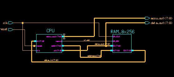
The CPU is connected to an external memory. The memory interface includes an 8-bit address bus, separate 8-bit read and write data buses, and a write enable line (wr_en) for writing to RAM
The CPU design includes the following internal 8-bit registers:
An asyncronous reset signal initializes all registers. After the reset is released, the program counter (PC) is set to a value corresponding to the default starting address of the program. When reset is released, the CPU reads and begins execution of the op-code stored at that memory address.
CPUs normally read and write to blocks of RAM. To simplify the design, you are provided with code that emulates an asynchronous memory in the FPGA logic. You may configure this ROM as you like.
The memory is initially loaded with the following program:
LDA 0x07
ADD 0x0A
STA 0x10
JNC 0x02
JMP 0x00
This program begins by loading the number 7 into the accumulator. It then adds the number residing in address '0A' to the number stored in the accumulator, and stores the result at address 0x10. If there is no overflow, jump to address 0x02 (where the ADD instruction is located), otherwise jump to the program start (address 0x00).
Here is the commented machine code as entered in the ROM:
|
address |
data |
comment |
|
00 |
01 |
code for LDA |
|
01 |
07 |
value 7 |
|
02 |
03 |
code for ADD |
|
03 |
0A |
address 0A |
|
04 |
02 |
code for STA |
|
05 |
10 |
address 10 |
|
06 |
04 |
code for JNC |
|
07 |
02 |
address 02 |
|
08 |
05 |
code for JMP |
|
09 |
00 |
address 00 |
|
0A |
09 |
Value 09 stored at address 0A |
VHDL description
Begin by creating a new, empty project. Download and add the following four VHDL files:
The architecture is not complete, as it only includes the LDA op-code and an internal read_opcode operation. You will need to expand the FSM with code for the other operations.
You may use the LDA code as a template for the other op-codes, although it is important to note that LDA requires only one clock cycle to execute. Other op-codes will require more than one clock cycles, and therefore multiple states in the FSM.
The ADD instruction may require more thought than the others, for two reasons: First, the value to be added to the accumulator is not immediately available after the op-code is decoded, because it must first be be read from the indicated memory location. The second reason stems from the carry flag. To add two 8 bit values, they should first be converted to 9-bit vectors and then added (in order to handle eventual overflows). The 8 least significant bits in the result should then be placed in the accumulator, and the most significant bit written to an "overflow" (or "carry") register. The instruction JNC ("Jump if No Carry") uses this last register to decide whether to jump to a new address.
The processor can be described as a state machine. The first state, "load_opcode", reads the instruction code from the memory and decodes it. Depending on the instruction that has been read in, the state machine will transition to the appropriate state to execute that instruction.
To simplify the instruction decoding, "load_opcode" evaluates only the four least significant bits on the data bus are decoded. This allows up to 16 instructions, which is completely sufficient for this exercise. If more instructions are eventually needed, you can increase the bit width used by the decoder.
The values for the different opcodes are defined in binary constant declarations in the CPU architecture.The CPU reads the memory contents from the dr port, and writes to the memory through the dw port. The contents of the current memory address are always available on dr, while the signal "wr_en" is used to write a new value the memory. The memory is written on the rising edge of the clock when wr_en is set to '1'.
Part 2: Implement and test in FPGA
After verifying your design in simulation, you can implement and test the design on your FPGA developer board.
Use one of the push buttons for reset, and connect the 7-segment display to the anode and cathode ports accordingly.The top level design uses two clocks: the CPU clock (clk) and the display clock (clk50). Use the 50 Hz oscillator input for the display clock, and a second push-button for the CPU clock. By pressing the button you can run the program step-by-step while following the program counter and accumulator values on the 7-segment display.
Part 3: Add something to the design
The processor as described up to this point is very simple, but it can be built out and extended in many different ways. Here is a list of possible extensions to the processor functions, some more simple than others. You can discuss other ideas with the instructor.
Additional op-code ideas:
Hardware peripheral ideas:
Appendix A. VHDL files for the processor